Results.
Faculty of Information Technology Department of Computer Engineering Digital Design (Schemotechnics) Report For laboratory work #1 “CMOS Logic Gates”
Written by: Kozhabekova A.S., FIT, IS, 1st year student Written to: Shamoi Pakita, Lecturer, CE, FIT
Almaty – 2013 Lab Report 1 – CMOS Logic Gates 1. Introduction to CMOS Logic. Logic gates are digital electronic circuits that perform some logic operations. These gates are widely used in making modern digital systems like phones, MP3-players, digital cameras. Logic levels are the voltage ranges for a 1 and 0. As the input and output of the gates will be a binary signal (0 or 1) these inputs will have logic levels that are 0V for a 0 and 5V for a 1. Logic gates are made up of switches that connect the output to the voltage for a 1 or 0. In this laboratory we use the switches called CMOS transistors. But there are other many different types of switches that can be used to build these logic gates. The CMOS transistors are of three terminals. There are source, drain and gate. Source is the terminal that is usually connected to a voltage source, drain is the terminal that usually connected to the output and gate is the input terminal. When a certain voltage is connected with the gate, gate will “turn on” the transistor and connect the drain to the source. There are NMOS and PMOS transistors.
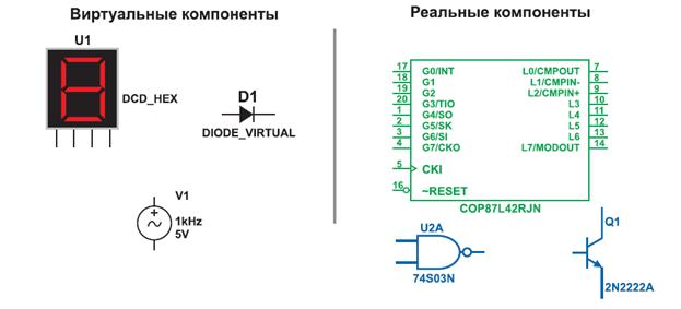
In Figure 3 we can see theCMOS (NOT) Gate Inverter. It is built by connecting a PMOS transistor to VDD (5V) or the logic 1 voltage. A NMOS transistor is connected to Ground or the logic 0 voltage. The drains and gates of the transistors are connected together. The input is connected to the gates. The output is connected to the drains.
Figure 4 shows the CMOS NAND (NOT AND) Gate Inverter. It is built by
the logic 1 voltage. Two NMOS transistors are connected in series to Ground or the logic 0 voltage. The drains of two PMOS and the top series NMOS transistor are connected to the output. The gates of one PMOS and one NMOS are connected to input 1. The gates of the other PMOS and other NMOS are connected to input 2.
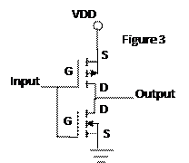
Results. 3.1a) Inverter (NOT) Gate: To build the circuit, I connected pin 8 to pin 13 with a wire. This is the output connection.
3.1b) NAND (NOT AND) Gate: To build the circuit, I connected pin 13 to pin 1, pin 2 to pin 14 (VDD), pin 8 to pin 4, and pin 5 to pin 1 with wires. Pin 1 is the output connection. Pin 6 is for input 1. Pin 3 is for input 2.
3.1c) NOR (NOT OR) Gate:
|
 The NMOS transistor is that transistor, which basic operation is that when the gate voltage is more positive than the source voltage. The PMOS transistor is, on the contrary, the transistor in which the gate voltage is more negative than the source voltage.
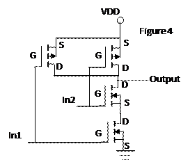 connecting two PMOS transistors to VDD (5V) or