Учитесь читать и переводить.
Текст 1.5. Прочитайте текст. Составьте прогноз содержания текста на основе ключевых слов. Озаглавьте текст.
Прочитайте текст еще раз и составьте его аннотацию на английском языке. Схема аннотации: 1. This review briefly surveys developments in the field of...; 2. It shows the advantages and disadvantages of...; 3. An attempt is made to deal with...; 4. Actually, the structure of the components permits...
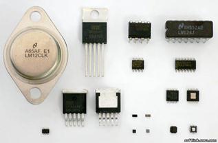
The potential of integrated circuits is so wide that in addition to replacing similar discrete component circuits they are responsible for creating a completely new technology of circuit design. There are two basic approaches to modern microelectronics – monolithic integrated circuits and film circuits. In monolithic ICs all circuit elements, active and passive, are simultaneously formed in a single small wafer of silicon. The elements are interconnected by metallic stripes deposited onto the oxidized surface of the silicon wafer. Monolithic IC technology is an extension of the diffused planar process. Active elements (transistors and diodes) and passive elements (resistors and capacitors) are formed in the silicon slice by diffusing impurities into selected regions to modify electrical characteristics, and where necessary to form p-n junctions. The various elements are designed so that all can be formed simultaneously by the same sequence of diffusions. Film circuits are made by forming the passive electronic component and metallic interconnections on the surface of an insulation substrate. Then the active semiconductor devices are added, usually in discrete wafer form. There are two types of film circuits, thin film and thick film. In thin film circuits the passive components and interconnection wiring are formed on glass or ceramic substrates, using evaporation techniques. The active components (transistors and diodes) are fabricated as separate semiconductor wafers and assembled into the circuit. Thick film circuits are prepared in a similar manner except that the passive components and wiring are formed by silk-screen techniques on ceramic substrates. There can be many instances where the microelectronic circuit may combine more than one of these approaches in a single structure, using a combination of techniques. In multichip circuits the electronic components for a circuit are formed in two or more silicon wafers (chips). The chips are mounted side by side on a common header. Some interconnections are included on each chip, and the circuit is completed by wiring the chips together with small diameter gold wire. Hybrid IC's are combinations of monolithic and film techniques. Active components are formed in a wafer of silicon using the planar process, and the passive components and interconnection wiring pattern formed on the surface of silicon oxide which covers the wafer, using evaporation techniques.
Текст 1.6. Прочитайте текст. Напишите его краткое содержание, используя модель: 1. The paper attempts to provide... 2....are discussed briefly. 3. They include... 4. The conclusion is as follows...
Integrated Circuit Development Three factors have contributed to the rapid development growth in the number of circuit elements per chip. One factor is improvement in techniques for growing large single crystals of pure silicon. By increasing the diameter of the wafers — the discs of silicon on which chips are manufactured — more chips can be made at one time, reducing the unit cost. Moreover, the quality of the material has also been improved, reducing the number of defects per wafer. This has the effect of increasing the maximum practical size of a chip because it reduces the probability that a defect will be found within a given area. The chip size for large-scale integrated circuits has grown from less than 10.000 square mils (thousandths of an inch) to 70.000. A second factor is improvement in optical lithography, the process whereby all the patterns that make up a circuit are ultimately transferred to the surface of the silicon. By developing optical systems capable of resolving finer structures, the size of a typical transistor, as measured by the gate length, has been reduced from a few thousandths of an inch in 1965 to two microns today. Finally refinements in circuit structure that make more efficient use of silicon area have led to a hundredfold increase in the density of transistors on the chip.
Текст 1.7. Переведите текст письменно без словаря. Значения выделенных слов вы сможете понять из контекста. Время перевода - 10 минут. Electronic Devices The invention of the transistor triggered the rapid growth of the electronics industry. Before transistors, electronic circuits were large, bulky and unreliable. They consumed considerable power (energy) and therefore generated too much heat, which contributed to the deterioration of other circuit parts and materials, such as resistors, capacitors and insulation. With transistors, circuits became much smaller, more efficient in the use of energy, and far more reliable. The higher reliability of the transistor circuits compared to vacuum tube equivalents is an extremely important advantage. The techniques used to manufacture transistors led to the development that made it possible to mass-produce very small and highly reliable electronics circuits commonly known as integrated circuits (ICs). ICs have diodes, transistors, resistors and all interconnecting leads formed on a single piece of semiconductor material.
Текст 1.8. Переведите текст письменно со словарем. Время перевода —15 минут. The Future of ICs When assessing the future course of ICs, it is customary to project another order of magnitude in circuit performance through a continuing reduction in the feature size of the devices on chip. However, at our current level of IC development we must face several pragmatic barriers that will require some degree of research creativity to overcome. For example, the chip complexity is extrapolated to 100,000,000 transistors per chip and beyond. However, the latest models indicate that the power level of next-generation devices will be on the order of 10 mW. Thus, a chip of this extrapolated complexity with these devices would require 1000 watts of input power and a packaging system capable of dissipating such power. Since these small devices would operate at reduced supply voltages, the 1000 watts of input power would require currents on the order of 200 amperes and perhaps greater on a chip that should be less than one square inch in area. This set of conditions would apply only to a high-duty cycle and high-performance design and points out that important complexity/performance trade-offs must occur. Conductors that are compatible with the device geometries must carry current densities much greater than the allowable limits defined by electromigration effects, resulting in a low reliability.
Определите контекстуальное значение выделенных слов. 1.24. Переведите, обращая внимание на контекстуальное значение выделенных слов pattern point; involve: 1. Optical lithography has been the leading integrated circuit pattern defining technique for many years. 2. In the narrow sense, pattern recognition means the classification of a given unknown pattern in into a number of standard classes. In broad sense, pattern recognition means scene analysis. 3. Electron beam changes physical characteristics of exposed resistor so that after chemical etchinig pattern is left on clear substrate. 4. Finished substrate may contain 10,000 mask patterns. 5. The amount of work done is movnig one coulomb of electricity from one point to another is a measure of the potential difference between these two points. 6. The principles involve preparing detailed plans and careful monitoring. 7. The circuitry and software involved can be standardized. 8. Plasma etching involves the use of a glow discharge. 9. This work has involved the contributions of many people.
МАТЕРИАЛЫ ДЛЯ САМОСТОЯТЕЛЬНОЙ ВНЕАУДИТОРНОЙ РАБОТЫ (ПОСЛЕ ВТОРОГО ЗАНЯТИЯ)
|


